Service provider in photonics since 2006
Like Jason and the Argonauts ventured into unexplored realms, the Argotech team is heading for new frontiers in semiconductor photonics and microelectronics.
About ARGOTECH
- Independent private company founded in 2006.
- Assembly and R&D service provider in optics, electronics and mechanics.
- Our capabilities are based on knowledge and skills from the time Siemens and Infineon set up their production in our region in the 1990s.
- Over 1000 square meters of ISO 7 and 8 class cleanroom premises.
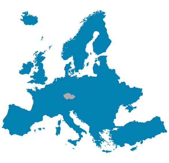
Argotech a.s. is a privately owned company ideally located in the heart of Europe in the Czech Republic. We specialize in assembly, development and engineering for fiber optics, semiconductor photonics, microelectronics and micromechanics.
We offer the complete back-end assembly process chain from wafer level to full optical assembly or customised semiconductor packaging solutions. We can support with 1pc prototyping or pilot production with the potential for rapid scaling up to volume production. Our R&D teams can provide feasibility studies, product design, prototyping, product qualification and process modifications.
OUR MISSION:
To provide continuous support for customers worldwide including manufacturing, development and engineering services focused on design, process development as well as expertise in optics, electronics and mechanics.
The Benefits Of Argotech
- European business approach focusing on quality and long term partnership.
- Smart solutions based on decades of experience in Czech Republic in electronics.
- We are a trusted and reliable partner in a demanding industry.
- We keep up to date with the latest developments thanks to our long-term partnerships with international scientific institutions, universities and world leaders in the business.
- Argotech is certified by ISO9001 since 2/2011.
Argotech is exclusively a service provider offering various semiconductor packaging platforms but does not market its own products.
The SERVICES we offer can be divided into three main groups:
- Manufacturing services
- R&D services
- Testing services
We prefer all the projects and contracts to be secured by a non-disclosure agreement.
For this reason, our references are practically limited to projects that we are allowed to publish. Please visit our REFERENCES for more information.
2022
New website design implemented.
2021
Started to implement digitalization elements into production processes.
2020
Most succesful year in our history in terms of overal turnover. Set up plan for investments in production and laboratory equipment.
2019
We are expanding the numbers of our colleagues.
2020
Nemo enim ipsam voluptatem quia voluptas sit aspernatur aut odit aut fugit, sed quia consequuntur magni dolores eos qui ratione
2017
Nemo enim ipsam voluptatem quia voluptas sit aspernatur aut odit aut fugit, sed quia consequuntur magni dolores eos qui ratione
2015
Nemo enim ipsam voluptatem quia voluptas sit aspernatur aut odit aut fugit, sed quia consequuntur magni dolores eos qui ratione
2011
Nemo enim ipsam voluptatem quia voluptas sit aspernatur aut odit aut fugit, sed quia consequuntur magni dolores eos qui ratione
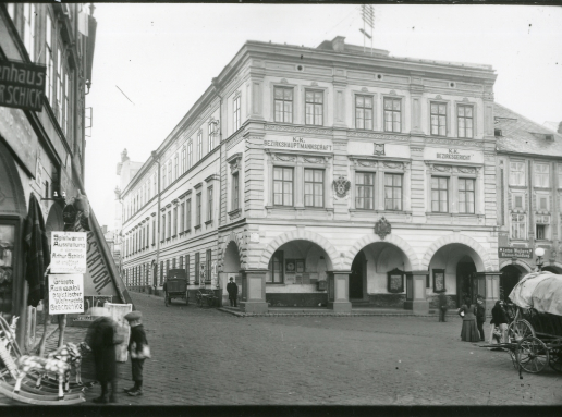
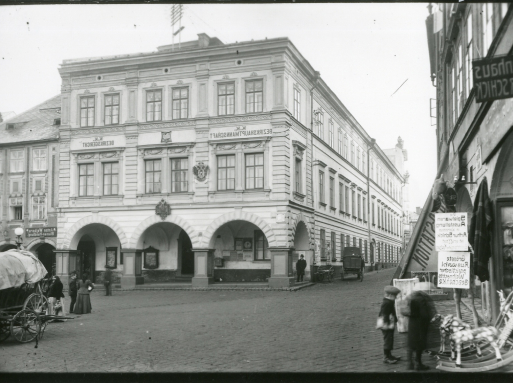
Our history
The company was founded in 2006 based on existing tradition of microelectronics available in the region after the restructuralization of Siemens and Infineon afterwards.

INDUSTRY
High-tech sensors
Durable data transfer

AUTOMOTIVE
LIDARs
Lighting

AEROSPACE
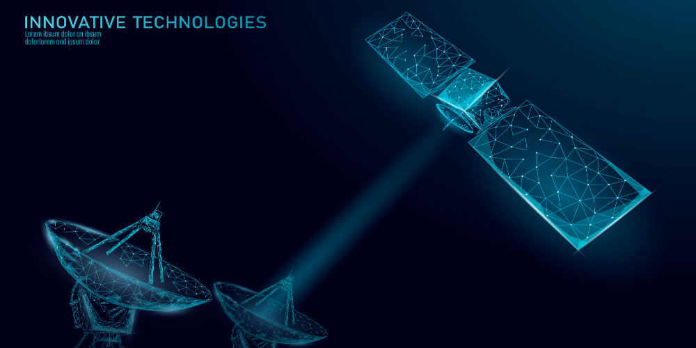
High speed data
Compact & Hermetic

HEALTHCARE
Non-invasive diagnostics
Life quality improvement
DEFENCE SECURITY
Detection
Durability

DATA TELECOM
Customized transceivers
Big data
History
2023
NEW TECHNOLOGY
Expanding the technology for precise hermetic assemblies in a protective atmosphere.
NEW TECHNOLOGY for R&D
Framework agreement signed to use equipment including PacTech Solder ball jetting, Zygo 3D profiler, Amtek Precise dispensing, Weiss Shock testing chamber.
2022
2021
NEW TECHNOLOGY
Complete technology upgrade for automatic Die-Attach process.
Advanced Sensing market
R&D and assembly support for LIDAR applications based on SiPh PIC chips.
2020
2019
TEAM EXPANSION
Recruiting new members to production, R&D and other supporting teams.
Silicon Photonics project
Silicon Photonics assembly and packaging technology improved and utilized in project PIXAPP within EU programme Horizon 2020, (see REFERENCES).
2017
2016
ENTERING the CERN project
NEW TECHNOLOGY
Flip-chip system upgrade enabling submicron placement accuracy for packaging of the newest chips.
2015
2014
First EU funded R&D project
With project ADDAPT we entered the European Union programme FP7-ICT,
(see REFERENCES).
QUALITY MANAGEMENT
Company ISO9001 certificated
by Bureau Veritas.
2011
2010
NEW PRODUCTION PREMISES
Construction of new production cleanroom premises and relocation.
NEW TECHNOLOGY
and equipment procured.
2008
2007
TEAM EXPANSION
Significant company development
and recruitment.
COMPANY ESTABLISHMENT
incorporation of joint-stock company
on 23rd May 2006
2006
Job offer
Nabídka zaměstnání
Zajímají vás nejnovější technologie? Chcete pracovat v úspěšné elektrotechnické společnosti?
Přidejte se do našeho týmu a získejte nové zkušenosti a znalosti v oblasti mikroelektroniky, přesné mechaniky a fotoniky.
Prohlédněte si nabízené pozice.