Manufacturing services
Complex assembly and packaging solutions for semiconductor photonics and microelectronics industries.
From wafer level assembly to transceivers and hermetic systems for aerospace.
Assembly and packaging capabilities
Wafer level assembly processes:
- Wafer level die-attach, wire bonding, sorting, soldering, burn-in, electro-optical measurements
- Precise dispensing of adhesives, solder pastes and other compounds
- Wafer dicing (silicon, ceramics or glass substrates dicing, bare die singulation)
Semiconductor component packaging processes:
- Complete die-attach process including pick & place,
- Wire bonding
- Active optical alignment,
- Hybrid integration,
- Hermetic sealing on traditional or customized packages and others as described below.
Typical application:
- Simple bare chip integration into TO-CAN or butterfly packages. Typically edge-emitting laser diode (LD), VCSEL, LED, photo diode (PD), photonics sensors, etc.
- Wafer level component sorting, die-bonding and wirebonding.
- Complex packaging solutions based on high-tech approaches combining various technologies such as Silicon Photonics including hybrid integration with flip-chip and solder bumping and optical alignment.
General parameters:
- WLA – wafer level assembly
- Component assembly (Bare die, COB – Chip-on-board)
- Flexible volumes
(from 1pc to serial batch) - Flexible assembly process complexity
(single chip to complex system) - Wide operating wavelength applications
(200nm – 20µm) - High frequency applications beyond 110GHz
- Traditional packaging TO-CAN packages
- Customized hermetic packages
- Advanced solutions based on high-tech approaches such as Silicon Photonics, including hybrid integration.
Our team of experts has over 20 years of experience in key assembly processes
such as die-attach, wire bonding and active alignment.
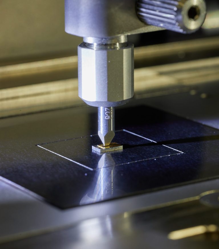
Die-Attach technologies
Description:
Die-Attach represents a wide technology group for component placement and attaching with adhesive, solder or other compounds.
Each group requires a specific approach, plus equipment, technology and skilled personnel.
We operate with a wide range of technologies that enable us to process traditional or high-tech components and offer the most efficient solutions. Especially the following:
- technologies for both face-up and face-down attach (flip-chip)
- bonding with UV, optical, thermal or electrical conductive adhesives
- soldering using hot tool or laser assisted local soldering
- thermo-compression using stud bumping
- solder ball jetting for ultra-high precision flip-chip applications
precise dispensing and stamping
Parameters:
- placement accuracy up to 0.5µm
- component (bare die) size from 150 x 150µm
Typical applications:
Laser diode attach on interposer, PIC attach, component sorting, EIC flip-chip on PIC
Wire bonding
Wire bonding has been the most commonly used method for component interconnection with substrate, PCB or package module. The most standard is the ball bonding with ball/wedge method. We can process also full ball stich on ball (BSOB) or wedge/wedge method.
Every year the components get slighlty smaller, so using the 17µm gold wire we can hit the ultra-fine bond pad pitch (BPP) even under 60µm. It means that together with placement accuracy +/-3µm we are able to provide wire bonding services of the newest components including the Photonic Integrated Chip (PIC).
Parameters:
- high speed or low volume batch
- wire material: gold or aluminium
- method: Ball/wedge, BSOB, wedge/wedge, ribbon wire
- ultra-fine bond pad pitch: from 60µm
- placement accuracy: ±3µm
- pull-test and ball-shear test according to MIL standards.
Typical application:
- Wafer level – Interconnect of chip to interposer
- Component level – Interconnect of sophisticated multichannel chip on substrate layout
Do you need more information?
We are ready to assist you. Contact us directly here and give us a brief description of your project. We will get back to you as soon as possible.
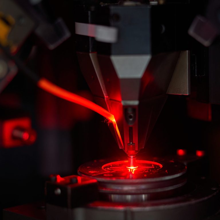
Active alignment / optical coupling
Active alignment is a key assembly process step ensuring successful photonic chip integration.
Every application requires a specific integration approach. For that reason we offer a wide range of active alignment approaches to meet specific product requirements.
Parameters:
- Free-space optic solutions
- Butt coupling, both edge emitters and grating couplers
- Tasks from 4 DOF to 6 DOF (Degree Of Freedom)
- Fixation techniques: laser welding for single channel applications, UV adhesive for multi-channel applications.
- Accuracy down to 20nm linear and 0.001 deg angular
Typical application:
- Fiber array block (FAB) to chip alignment
- Pigtail to butterfly or TO-CAN alignment
- Microlens alignment (focusing and collimation)
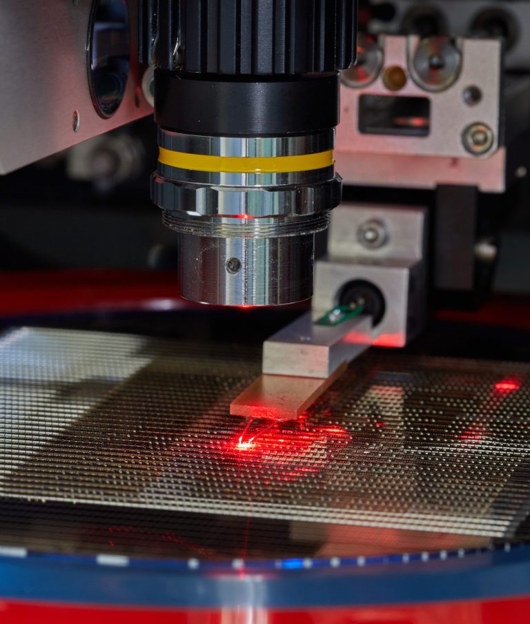
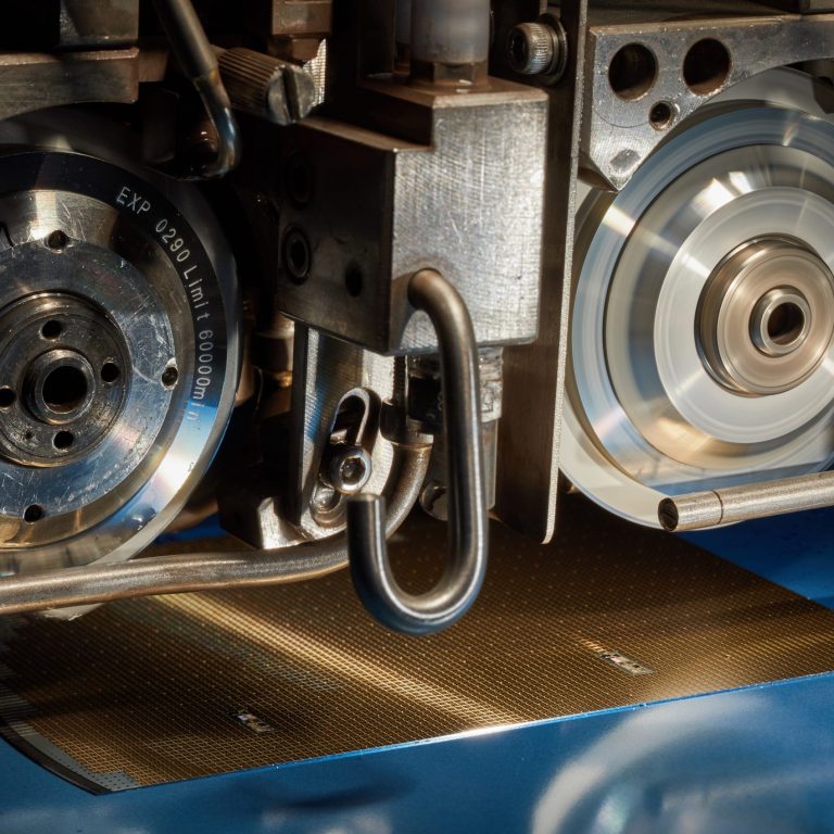
Solder bumping and other soldering processes
Soldering processes are essential for good thermal management of bonded chips. Most critical are the laser chips and the SOA chips. There is a chain of technologies necessary for this process group.
Parameters:
- solder preforms
- solder jetting, ball size 60 – 400µm, wafer scale application
- local reflow by hot-tool or laser assisted soldering
- reflow in specific ovens multi-zones, vacuum oven, specific atmosphere ovens
Typical application:
- Chip on submount soldering, flip chip
- Lid soldering
Do you need more information?
We are ready to assist you. Contact us directly here and give us a brief description of your project. We will get back to you as soon as possible.
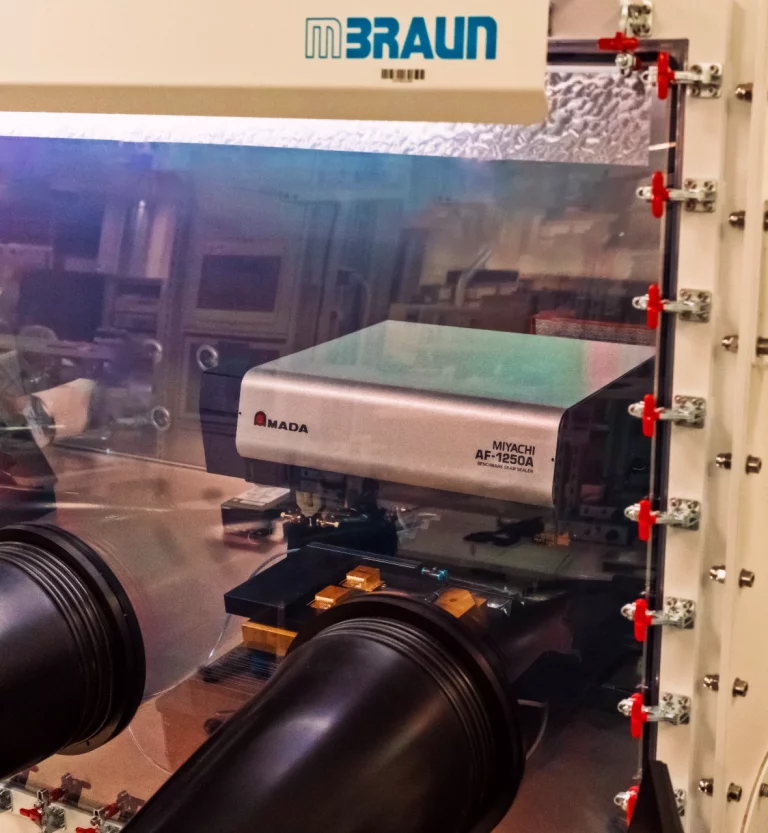
Hermetic sealing
and encapsulation
Hermetic sealing is an essential process for providing a stable environment for sensitive semiconductor chips especially the photonics ones. It is necessary to keep the stable environment conditions typically to protect the chips from the oxygen which mostly heads to rapid ageing of the chips. Furthermore the optical subassemblies are sensitive to humidity which impacts the optical paths.
Parameters:
- Various types of atmosphere
- Nitrogen or specific mixtures of gases
- Welding and soldering approaches
- In specific cases lid glueing process with dedicated glues
- Fine and gross leak test
Typical application:
- Cap welding for TO-CAN
- Cap soldering on specific carriers like alumina or silicon
- Lid seam sealing for butterfly packages
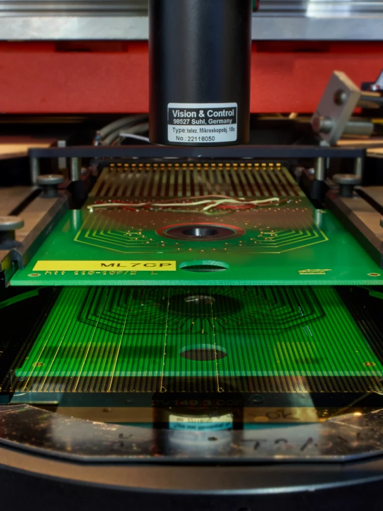
Inter-process verification - PBI
In order to guarantee a high process yield it is necessary to support it by inter-process verifications which provide the necessary feedback. Typically this involves a wide range of the visual inspections, statistical process control, and electrical and optical measurements.
Parameters:
- Shear test and pull test
- Automatic visual inspection systems, including wafer level capability
- Resolution 0.5µm
- Surface contact free profile meter, roughness and chip tilts, thicknesses etc.
Do you need more information?
We are ready to assist you. Contact us directly here and give us a brief description of your project. We will get back to you as soon as possible.
Testing and Burn-in
Electronic and photonic chips require initial stress testing which can eliminate the weak components and only pass the good chips for long durability in applications. This stress is known as burn-in process. It is essential to perform the burn-in as soon as possible in an assembly flow in order to save the material assembly costs in case the chip fails.
Evaluation if the chip is good can be achieved by the set of the electro – optical measurements.
Parameters:
- Wafer level carrier and die level testing and burn in
- LIV, spectrum and others
- Dry burn-in and biased temperature and humidity burn in
Supporting processes
There is another group of additional processes that ensure the production line remains flexible to meet specific requirements while delivering high quality, reliable and sustainable outputs.
This group includes dicing processes, for example, including laminating and delaminating, adhesives and other compounds preparation processes, dispensing, rework, analysis and other quality ensuring processes, etc.