Advanced semiconductor photonics assembly
We are a one stop service provider for design, assembly and packaging in semiconductor photonics and microelectronics.
We illuminate your path at every step from the concept to mass production,
covering all aspects: design, simulations, prototyping, testing, qualification, production…
Competencies

Our Business
Core Competencies
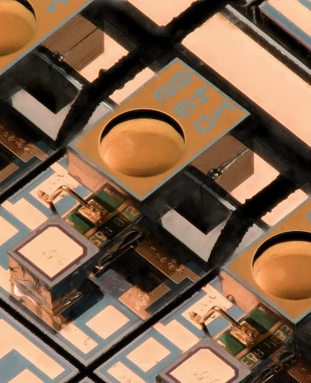
- Complex assembly and packaging solutions for semiconductor photonics and microelectronics industries.
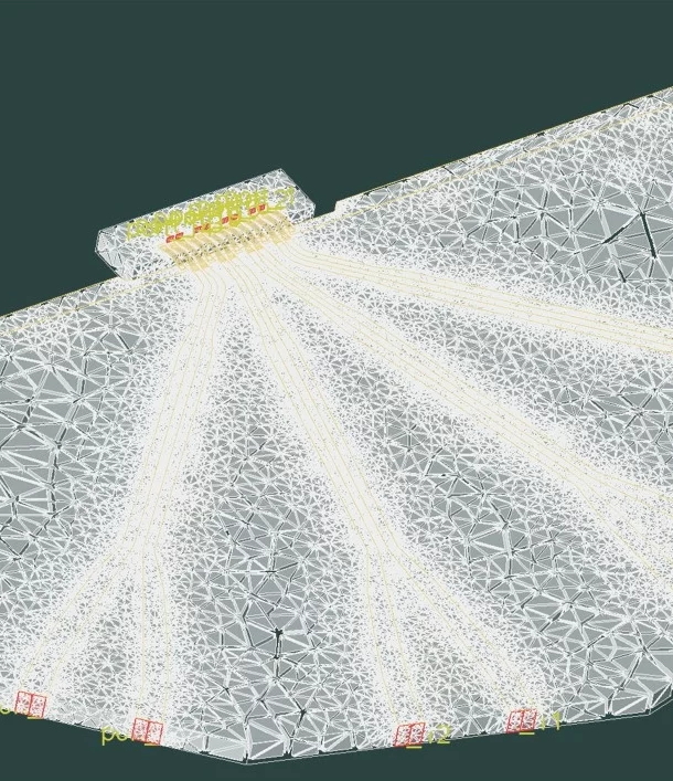
- Extensive experience with specialized simulation tools to design customized packages meeting thermal, optical and high frequency requirements.
- Advanced solutions based on high-tech approaches such as Silicon Photonics, including hybrid integration.
- Traditional solutions for bare chips integration in TO-CAN or butterfly packages.
- Experience in wide multispectral applications UV-VIS-NIR-MIR (200nm – 20µm).
- Design, prototyping, testing, qualifications for a variety of markets including sensing (LIDARs), healthcare (non-invasive diagnostics) or quantum photonics
OUR MISSION:
To provide continuous support for customers worldwide including manufacturing, development and engineering services focused on design, process development as well as expertise in optics, electronics and mechanics.
Solutions
Silicon Photonics
- The next level of integrated photonics entering a new era of application for use in everyday life.
- We provide complex integration capabilities:
-
- butt coupling of the fiber array to a chip (both edge and grating)
- free space optics coupling based on the lenses
- chip to chip coupling
- hybrid integration (EIC, III-V)
-
- We have been active in this field since 2017.

Assembly

Services
Assembly and Packaging
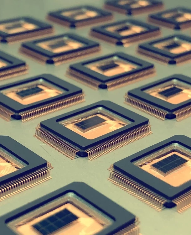
- Advanced assembly and packaging services for semiconductor photonics components in our own cleanrooms located in the EU, in the Czech Republic.
- Flexible production volume capacities from single piece to higher volume batches.
- Optional product complexity from single chip packaging to the complex device packaging.
- Available models of cooperation: CM, OEM and ODM.
- Wafer Level Assembly and component level assembly including Burn-in process.
- Advanced production data management in own database systems.
- Extensive engineering experience in manufacturing processes.
Silicon
Photonics
Photonics
Design
Services
Design and Qualification
- We are able to provide valuable feedback to front-end chip designers to enable efficient chip integration into the packages.
- We are here to support designers with integration into other subsystems and packaging modules and help to bring them to the market.
- We have a many years experience in packaging services designing the most efficient packaging for a wide range of applications.
- We support the design activities with high-tech simulation tools and an experienced engineering team.
- We help customers with qualification of photonics chips by accelerated ageing tests.

Our Services
and Technologies
- Our technology can be used either as a complete assembly process or only partially.
- Take a look at our R&D capabilities, where we can bring your idea to life.
- We can provide Proof of Concept data on your prototype
to determine if it is worth improving. - We can offer characterisation and testing devices for your production or research and development if you lack these capabilities.
Manufacturing
- Flexible volumes
- CM/OEM/ODM
- UV to MIR applications
- SiPh into TO package
- Complex packaging solution
- WLA and Component level Assembly
- PFMEA/Traceability/SPC
- Production data management
R&D services
- Simulations
- Feasibility study
- Packaging design
- Prototype builds
- Assembly process development
- Sample batch evaluation
- Publicly funded projects
- Long-term R&D contracts
Testing services
- Characterization
- Qualification
- Burn-In
- Enviromental tests
- Shock temperature tests
- Accelerated ageing
- Selected standards compliance test
- Long term endurance tests
Check out our latest company video
Job opportunities
Would you like to learn more about the latest trends in optoelectronics and work in a young team in a high-tech company? Check out the job opportunities here.
Benefits of
Argotech
Argotech

About us
Features and Benefits
Like Jason and the Argonauts ventured into unexplored realms, the Argotech team is heading for new frontiers in photonics and microelectronics.
- European independent private company founded in 2006.
- Assembly and R&D services provider in optics, electronics and mechanics.
- European business approach focusing on quality and long-term partnerships.
- Technically skilled personnel based on years of regional experience in electronics.
- We highly value agreements with our customers and strive to remain a reliable partner in a challenging industry.
- Over 1000m2 of ISO 7 and 8 class cleanroom production area.
- Argotech is certified by ISO9001 since 2/2011.
News
News & Events
20
Jun
W3+ Fair Jena 2025
Visit our booth no. G7 in Hall3 in Jena.Date: 24 + 25 September 20259.30 AM - 5.00 PM Sparkassen Arena Jena, GermanyDiscover the technologies of the f...
11
Dec
Laser World of Photonics 2025
Visit us on Laser World of Photonics 2025 in München in June 24th - 27th.Our booth with no. 434 located in Hall A2.Laser World of Photonics provides a...
