
PICTURE
Advanced material bonding to revolutionise photonic integration
High Performance and High Yield Heterogeneous III-V/Si Photonic Integrated Circuits using a Thin and Uniform Bonding Layer
Project ID: 780930
Start date: 1. 1. 2018
End date: 31. 12. 2021
EU cordis link: CORDIS
Website: picture-h2020.eu
Argotech’s role
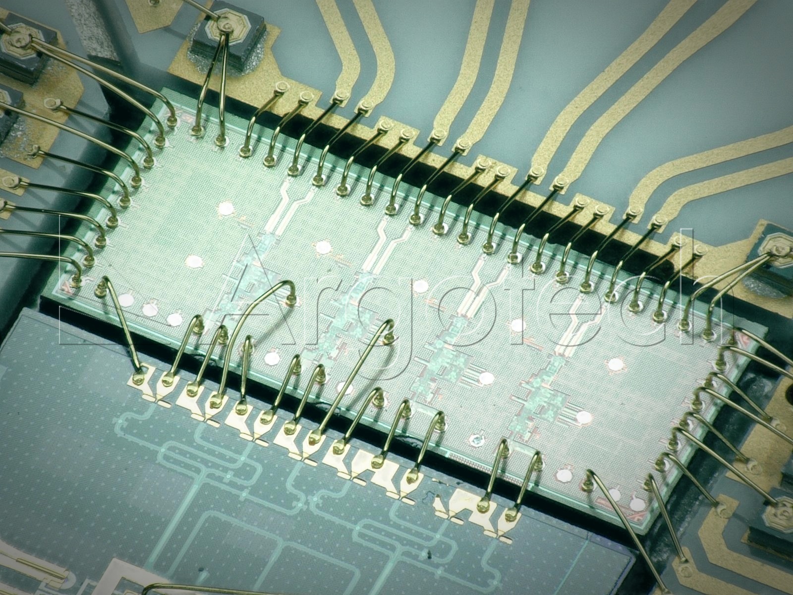
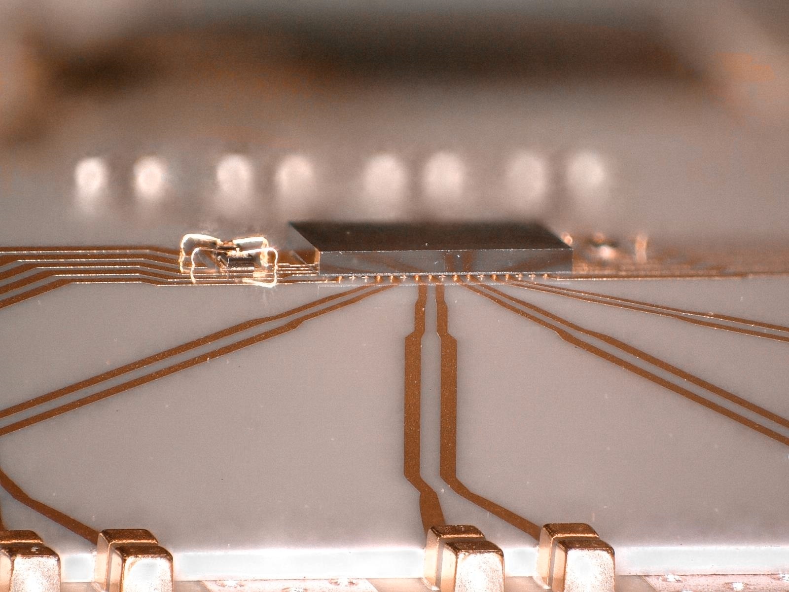
Designing and developing: the eletrical assembly, PCB design rules setting, HF design of fanouts in thin layer technology, simulation and optimalization.
Project description
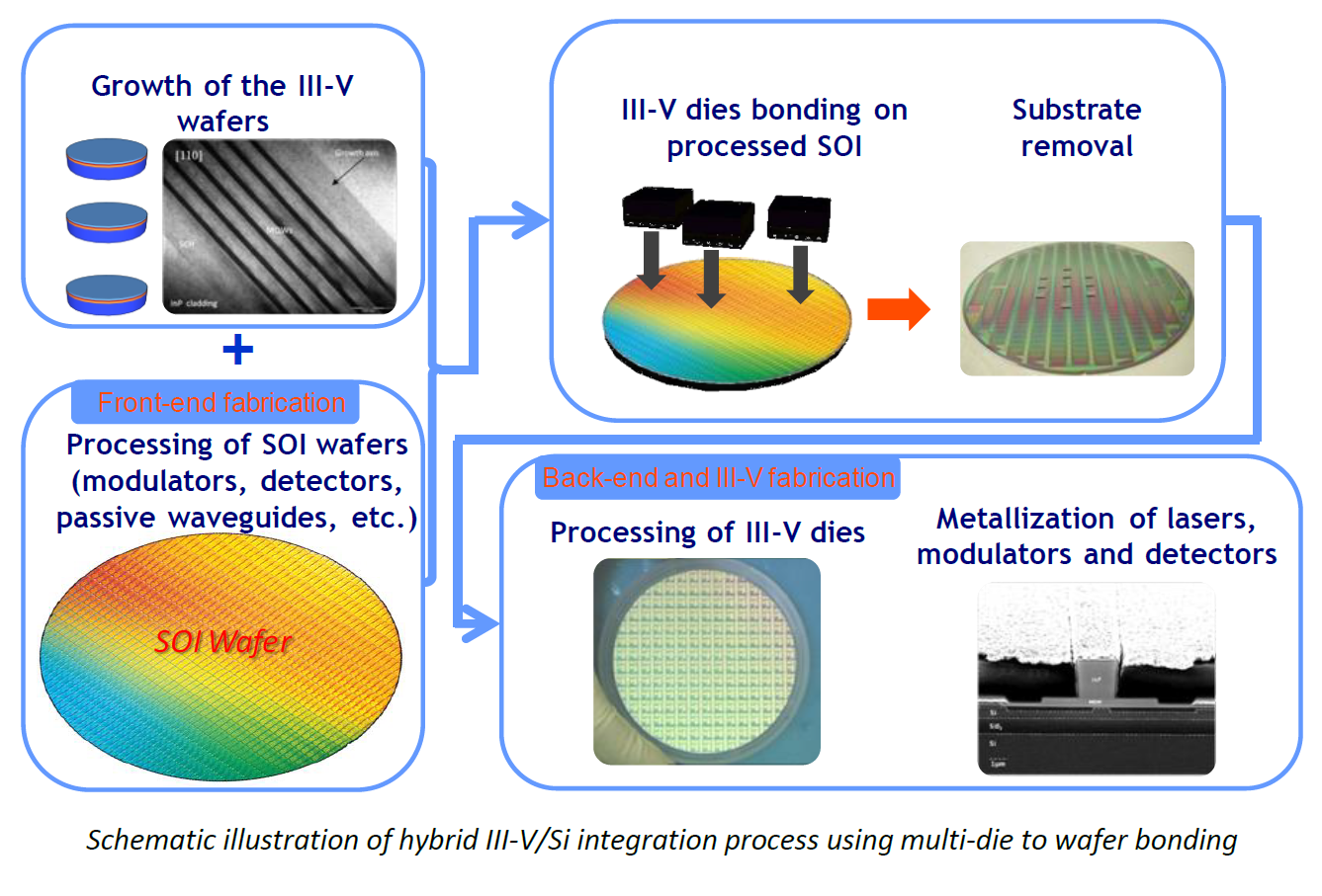
Photonic integration technology combines various components such as lasers, modulators and detectors on a single chip.
The EU-funded PICTURE project aims to develop advanced photonic integration technology by bonding multiple semiconductor dies made from III-V compound materials to silicon-on-insulator wafers. This heterogeneous integration platform will enable higher-performance lasers, photodetectors, MOSCAP III-V/Si modulators and distributed feedback lasers with tuneable wavelength.
The entire process will be executed on a 200-mm R&D CMOS line, resulting in higher yield, smaller footprint, and lower-cost photonic integrated circuits (PICs). Furthermore, PICTURE will develop quantum-dot lasers by directly growing them on bonded templates, aiming to enhance the performance of future high-density PICs.
Objective
The objective of PICTURE project is to develop a photonic integration technology by bonding multi-III-V-dies of different epitaxial stacks to SOI wafers with a thinner and uniform dielectric bonding layer. This heterogeneous integration platform will enable higher performance lasers and photo-detectors using the optimized III-V dies.
In addition, the thinner bonding layer will lead to record performance MOSCAP III-V/Si modulators, and to a new generation of wavelength tunable distributed feedback lasers.
Moreover the full process including SOI process, bonding, III-V and back-end process will be made on a 200mm R&D CMOS line, leading to higher yield, smaller footprint and lower cost PICs. Two types of PICs with a total capacity of 400Gb/s will be developed, packaged and validated in system configuration.
In parallel, PICTURE project will develop direct growth of high performance quantum-dot lasers and selective area growth on bonded templates for high density future generation of PICs.
The project is coordinated by III-V Lab, and includes University of Southampton, CEA, University College London, Imec, Tyndall, Argotech and Nokia Bell Labs. The consortium is highly complementary, covering all skills required to achieve the project objectives: growth of semiconductor materials, silicon process and III-V process, design and characterization of PICs, prototyping and assessment of PICs in high bit rate digital communication systems.
Apart from the adequacy of the consortium to achieve collectively the project objectives, the consortium partners have the potential to set up a comprehensive supply chain for the future exploitation of the project results, either by exploiting the results “in house” or by setting up suitable partnerships.
Coordinator:
III-V LAB, France
Partners:
CEA LETI – Commissariat a l’Energie Atomique et aux Energies Alternatives, France
IMEC – Interuniversitair Micro-Electronica Centrum, Belgium
Nokia Networks France, France
Tyndall National Institut, University College Cork, Ireland
University College London, United Kingdom
University Of Southampton, United Kingdom
This project has received funding from the European Union’s Horizon 2020 research and innovation programme
under grant agreement no. 780930.

